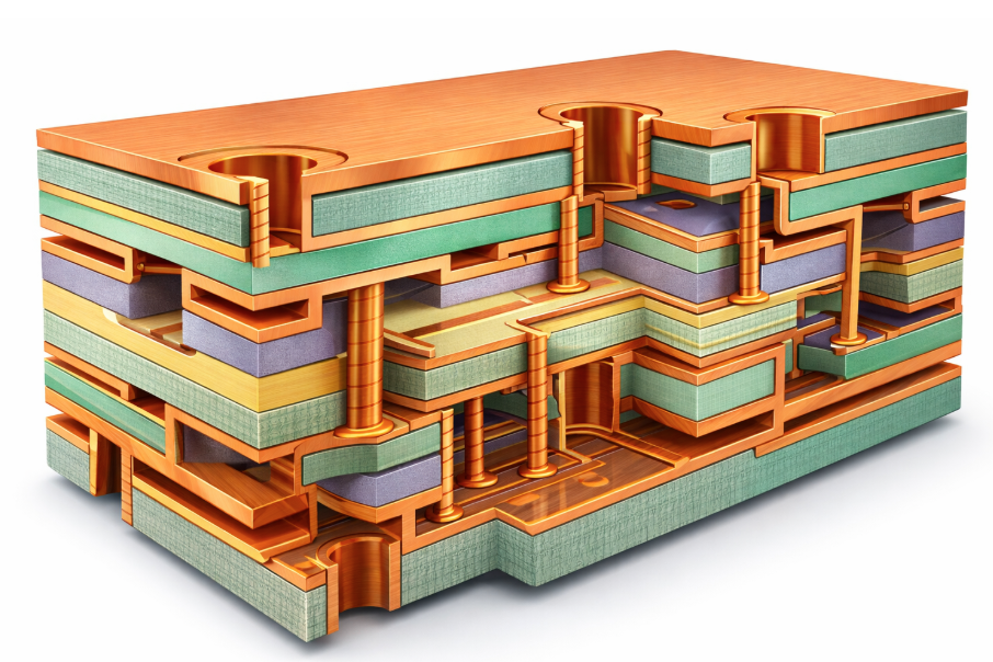
A multilayer HDI PCB combines the routing depth of multilayer board construction with the high density interconnect technologies that make modern compact electronics possible. Where a standard multilayer board routes signals through mechanical through-holes that pass across every layer, an HDI multilayer design uses laser-drilled microvias, blind vias, and buried vias to connect layers selectively. The result is a board that carries more signals, fits more components, and performs better electrically in a fraction of the space.
Designing and manufacturing multilayer HDI boards correctly requires understanding both disciplines. The stack-up decisions you make at the design stage determine whether the board is manufacturable, what it costs, and how reliably it performs in the field. This article covers the design rules that matter most, the manufacturing considerations that follow from those decisions, and the specifications you need to confirm before placing an order.
What a Multilayer HDI PCB Is
A multilayer PCB is any board with more than two copper layers. Standard multilayer boards typically range from 4 to 12 layers for commercial applications, with telecom, server, and automotive designs running to 16, 20, and higher layer counts. All layers in a standard multilayer board are drilled and plated in a single production cycle, and through-holes connect layers across the full board thickness.
An HDI multilayer board adds high density interconnect capability on top of the multilayer foundation. Instead of relying exclusively on through-holes, the HDI design uses microvias to connect only adjacent layers, blind vias to connect outer layers to selected inner layers, and buried vias to connect inner layers to each other without consuming space on the outer surfaces. These vias are formed by laser drilling and sequential build-up lamination rather than a single drill-and-plate cycle.
The combination matters because it unlocks routing density that neither approach achieves alone. A multilayer stack gives you the number of routing layers you need for complex circuits. HDI via technology gives you the interconnect density to escape high pin count BGAs, route 0.4 mm pitch packages, and reduce board area by over 30 percent compared to an equivalent standard multilayer design.
FastTurn PCB supports multilayer HDI builds from 4 layers up to 32 total layers with up to 18 HDI build-up layers. Stack options include 1+N+1, 2+N+2, 2+2+N+2+2, and any-layer structures. Controlled impedance is held to within plus or minus 5 ohms, and high-speed differential signaling up to 28 Gbps is supported.
See also: Homerocketrealty .Com: Homerocketrealty.Com: Exploring Digital Real Estate
Stack-up Design: The Foundation of Every HDI Multilayer Board
The stack-up is the cross-sectional layer arrangement of the board. It defines which layers carry signals, which carry power and ground, how thick the dielectric is between each pair of adjacent layers, what copper weight is on each layer, and where the build-up layers sit relative to the core. Every important electrical and mechanical property of the finished board flows from the stack-up.
Layer assignment
Signal layers, power planes, and ground planes need to be assigned before routing begins. The most reliable approach for high-speed multilayer HDI designs is to pair every signal layer with a solid reference plane immediately adjacent to it. This keeps the return current path close to the signal path, minimizes the loop area, and controls impedance. Avoid routing signals across split planes because the discontinuity in the return path creates EMI and signal integrity problems.
For a typical 8-layer HDI board, a common assignment is: Layer 1 signal, Layer 2 ground, Layer 3 signal, Layer 4 power, Layer 5 ground, Layer 6 signal, Layer 7 ground, Layer 8 signal. This arrangement keeps every signal layer adjacent to a solid reference and distributes the power and ground planes symmetrically through the stack.
Symmetrical construction
Every multilayer stack-up should be symmetrical about the center of the board. If the top half of the stack has a 1 oz copper layer on a 4 mil dielectric, the bottom half should mirror that arrangement. Asymmetrical stacks create uneven thermal expansion stresses during lamination and reflow, which causes board warpage. Warped boards cause assembly problems and field reliability issues. FastTurn PCB engineers review your stack-up for symmetry during DFM and will flag asymmetrical constructions before production begins.
Dielectric thickness and impedance
The thickness of the dielectric between a signal layer and its reference plane, combined with the trace width and copper weight, determines the characteristic impedance of routed traces. For standard single-ended signals targeting 50 ohm impedance, typical trace widths on inner layers of a standard FR4 stack with 4 mil dielectric run around 8 to 9 mil. For differential pairs targeting 100 ohm differential impedance, trace widths are narrower and spacing between the pair is tighter.
On HDI build-up layers, the dielectric is much thinner than on core layers, typically 2 to 4 mil. Thinner dielectric means narrower traces are needed to hit the same target impedance, which is one reason HDI layers use 2.5 to 3 mil trace widths rather than the wider traces used on inner core layers.
Always define your target impedance values and specify which signal layers they apply to in your stack-up document. FastTurn PCB will calculate the trace geometry needed to hit your targets and confirm it during DFM review.
Core and build-up layer arrangement
In a 1+N+1 HDI stack, the core carries N standard multilayer inner layers, and one HDI build-up layer sits on each side of the core. The build-up layers are the outermost layers and carry the finest traces and the microvia structures. Components mount directly on the build-up layer surface.
In a 2+N+2 stack, two build-up layers on each side allow more routing channels near the surface. This is needed for very high pin count BGAs where a single build-up layer does not provide enough routing channels for the via escape. The tradeoff is two sequential lamination cycles on each side instead of one, which increases fabrication cost and lead time.
In a 2+2+N+2+2 stack, four build-up layers on each side are available. This level of HDI density is used in the most complex designs, such as processors with thousands of BGA balls or boards with multiple stacked memory packages. Any-layer HDI, where every layer is a build-up layer, represents the maximum achievable density and is used in smartphone motherboards and similar ultra-compact designs.
Via Design Rules for Multilayer HDI Boards
Via design is where most HDI design errors originate. The rules below reflect manufacturing reality, not theoretical limits.
Microvia aspect ratio
A microvia should not be deeper than it is wide. The recommended maximum aspect ratio is 1 to 1, meaning a 100 micrometer diameter microvia should connect layers no more than 100 micrometers apart. This ratio ensures the via walls can be plated with uniform copper thickness from top to bottom. Exceeding a 1 to 1 aspect ratio makes it progressively harder to get plating solution into the via and results in thin or voided plating at the bottom of the hole, which is a reliability failure mode.
In practice, this means your dielectric thickness between build-up layers must be matched to your microvia diameter. FastTurn PCB uses dielectric thicknesses in the 2 to 4 mil range for build-up layers, which is well matched to 100 micrometer microvias.
Stacked versus staggered microvias
When two build-up layers are present on one side of the board, the microvia in the outer layer can either stack directly on top of the microvia in the inner build-up layer, or shift its position. Stacked microvias save board space because the two vias occupy the same footprint on the board surface. Staggered microvias use more surface area but are significantly easier to manufacture reliably.
The manufacturing concern with stacked microvias is stress concentration. During thermal cycling, the stacked structure expands and contracts vertically. The top via puts direct compressive and tensile stress on the bottom via, and if the bottom via plating has any weakness, it will crack. Industry guidance is to avoid stacking more than three microvias vertically and to use staggered or skip vias where possible. FastTurn PCB recommends staggered structures for prototype builds and accepts stacked structures with a DFM discussion for designs where space constraints require it.
Via in pad
Via in pad places a microvia directly on a component pad rather than adjacent to it. This is necessary for BGA packages with 0.4 mm pitch or below, where there is not enough space between pads to route a via beside the pad. At 0.5 mm pitch, via in pad is optional but often used to improve routing density.
Via in pad requires filling and planarizing the via before soldermask and surface finish are applied. An unfilled via in pad allows solder to wick into the via barrel during reflow, creating a void under the BGA ball and a cold or weak joint. FastTurn PCB fills via in pad structures with copper or epoxy and planarizes the surface to within 10 micrometers, providing a flat, solderable pad that behaves the same as a solid copper pad during assembly.
Buried via design
Buried vias connect inner layers to each other without appearing on the outer surface of the board. They are drilled and plated before the outer layers are laminated over them. The practical benefit is that buried vias free up outer layer routing space and allow inner layers to be densely interconnected without consuming through-hole space.
The manufacturing constraint on buried vias is that they must be formed during an inner-layer lamination step before the outer build-up layers are added. This means your design must specify clearly which inner layers the buried via connects, and the stack-up must be arranged so those layers can be laminated and drilled as a sub-assembly before the outer layers are added. A buried via that is not achievable in the planned lamination sequence will require a stack-up redesign.
Minimum annular ring
The annular ring is the copper ring surrounding a via hole on the pad. For microvias, the minimum pad diameter at FastTurn PCB is 200 micrometers for a 100 micrometer via, giving an annular ring of 50 micrometers on each side. For plated through-holes, the minimum finished hole diameter is 0.15 mm with a minimum pad diameter that maintains the annular ring within the layer-to-layer registration tolerance.
If annular rings are too narrow, layer-to-layer misregistration during lamination can break the ring and open a connection. FastTurn PCB holds layer-to-layer registration within 50 micrometers, which is the tolerance your pad dimensions must accommodate.
Trace and Space Design Rules
Minimum trace width and space on HDI build-up layers
FastTurn PCB produces HDI build-up layers with a minimum trace width and space of 2.5 mil each. This is the production minimum, which means it is achievable with consistent yield. Designing at exactly the minimum is not recommended because yield drops as you approach the process edge. For most HDI designs, 3 mil trace and space on build-up layers is more practical and will produce better yield than 2.5 mil.
Reserve 2.5 mil trace and space for BGA escape routing and other areas where the space is genuinely constrained. On inner core layers where you have more room, use wider traces. 4 to 5 mil on inner layers is common and produces excellent yield.
Differential pair routing
High-speed differential pairs need to be routed with matched lengths between the positive and negative traces. Any length mismatch introduces skew, which degrades signal quality. FastTurn PCB recommends keeping differential pair length mismatch within 5 mil for signals operating above 1 Gbps, and within 2 mil for signals above 10 Gbps.
Keep differential pairs on the same layer. Transitioning a pair between layers using vias introduces stub length and impedance discontinuity that degrades signal integrity at high data rates. If a layer transition is necessary, use a pair of microvias placed as close together as possible and keep the transition length minimal.
Clearance to board edge
Copper must maintain minimum clearance to the board edge to prevent shorts after routing and to avoid exposing copper at the cut edge. FastTurn PCB requires a minimum of 0.3 mm clearance from copper features to the board edge for routed boards. For scored boards, 0.5 mm is recommended.
Materials for Multilayer HDI Boards
Material selection for multilayer HDI designs depends on the operating frequency of your signals, the thermal environment the board will see in service, and any regulatory or environmental compliance requirements.
High Tg FR4
The standard material for multilayer HDI production. High Tg laminates withstand the thermal stress of multiple sequential lamination cycles and multiple reflow passes during assembly without delamination or excessive z-axis expansion. FastTurn PCB uses high Tg FR4 as the default for all multilayer HDI builds.
Halogen-free laminates
Required for automotive OEM supply chains, many industrial applications, and products sold in regions with strict environmental regulations. Halogen-free materials meet IEC 61249-2-21 and provide comparable electrical performance to standard FR4. FastTurn PCB stocks halogen-free options for both core and build-up layers.
Mixed dielectric for high-speed designs
At signal frequencies above 5 to 10 GHz, the signal loss in standard FR4 becomes significant. The copper roughness of FR4 laminates also contributes to skin effect losses at these frequencies. For boards with SerDes channels operating at 10 Gbps and above, a mixed dielectric stack-up is worth considering. Signal-critical layers use low-loss laminate with smoother copper foil. Layers carrying power, ground, and lower-speed signals use standard FR4. This approach provides the necessary electrical performance on the layers where it matters while keeping material cost lower than an all-low-loss build.
Resin Coated Copper for build-up layers
Build-up layers in HDI construction use Resin Coated Copper or laser-drillable prepreg rather than the glass-fiber prepreg used between core layers. These materials are thinner, more uniform in thickness, and easier to laser-drill than glass-reinforced materials. RCC provides precise control over dielectric thickness, which translates directly to better impedance control on build-up layer traces.
What Affects Cost on a Multilayer HDI Board
HDI multilayer boards cost more than standard multilayer boards because the manufacturing process is more involved. Understanding the cost drivers helps you make informed trade-offs during design.
- Layer count: More layers mean more lamination, drilling, and plating steps. Each additional layer pair adds cost. Use the fewest layers that achieve your routing requirements.
- Number of sequential build-up cycles: Each build-up cycle adds a full lamination, laser drilling, and plating sequence. A 1+N+1 structure costs less than 2+N+2, which costs less than 2+2+N+2+2. Minimize build-up cycles to the number genuinely required by your routing.
- Via in pad: Via fill, planarization, and replating add process steps and cost. Use via in pad only where the component pitch requires it.
- Buried vias: Buried vias require inner-layer lamination and drilling as a separate process step before outer layers are added. Each distinct buried via layer pair adds cost.
- Controlled impedance: Adds TDR testing and coupon processing. Necessary for any design with high-speed differential pairs, but adds cost per panel.
- Specialty materials: Halogen-free, low-loss, and mixed dielectric stack-ups cost more than standard high Tg FR4. Use specialty materials only on layers where performance requires it.
Working with FastTurn PCB on Multilayer HDI Projects
FastTurn PCB has built multilayer HDI boards across medical, automotive, telecom, server, and consumer electronics applications since 2015. Their capability covers 4 to 32 total layers with up to 18 HDI build-up layers, microvias down to 100 micrometers, trace and space down to 2.5 mil, and controlled impedance to within plus or minus 5 ohms.
Every multilayer HDI order receives a DFM review before any material is ordered or laminated. Engineers check your stack-up for symmetry and manufacturability, verify that your via aspect ratios and annular rings are within the process window, review your impedance specifications against your trace geometry, and flag any stacked via structures that carry reliability risk. This review is free and returns feedback same day for most designs.
Prototype quantities of multilayer HDI boards ship in 3 to 7 business days depending on layer count and complexity. Production quantities are quoted with lead times confirmed at order placement. There is no minimum order quantity.
Boards are inspected to IPC-A-600 and IPC-6012 standards. Assemblies follow IPC-A-610 Class 2 or Class 3. Certifications include ISO 9001, ISO 13485, UL, RoHS, and REACH.
Common Questions on Multilayer HDI Design
How do I know if my design needs HDI or if a standard multilayer board will work?
The answer comes down to your component footprints and routing density. If your design includes BGA packages with 0.5 mm pitch or below, or if you cannot complete routing in the number of layers you need with standard through-hole vias, HDI via technology will help. If all your components have 0.8 mm or wider pitch and your routing completes on a standard stack-up, a standard multilayer board is more cost-effective.
Can I mix HDI layers with standard inner layers in the same board?
Yes. A 1+N+1 or 2+N+2 structure is exactly this. The N core layers are standard multilayer inner layers processed in a single lamination cycle. The build-up layers on the outside are HDI layers added in sequential lamination cycles. The two approaches are designed to work together.
What is the fastest turnaround available for multilayer HDI prototypes?
FastTurn PCB delivers 1+N+1 HDI prototype builds in 24 to 48 hours when files are complete and materials are in stock. More complex 2+N+2 and higher structures take 5 to 7 business days for prototypes. Production quantities have lead times quoted at order placement.
Do I need to specify my stack-up, or will FastTurn PCB design it for me?
You should provide a stack-up specification that defines the layer sequence, dielectric material and thickness, copper weight, and finished board thickness. If you do not have a stack-up designed, FastTurn PCB engineers can propose one based on your layer count, impedance requirements, and material preferences during the DFM review.
Conclusion
Designing a multilayer HDI PCB successfully requires making the right decisions at the stack-up stage before routing begins. Symmetrical construction, proper layer assignment with reference planes adjacent to every signal layer, via aspect ratios within the 1 to 1 limit, and trace widths that stay above the process minimum rather than at it are the rules that separate boards that work from the first build from boards that require multiple revision cycles.
Manufacturing a multilayer HDI board successfully requires a supplier with verified laser drilling capability, sequential build-up lamination experience, and a DFM process that reviews your design before production starts rather than after the first build fails inspection.
To get a stack-up review and quote for your next project, visit multilayer HDI PCB manufacturing at FastTurn PCB and upload your files for a same-day DFM review.